About the opportunity
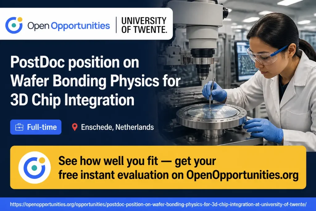
Wafer-to-wafer bonding is a key enabling technology for future 3D chip integration, where chips are stacked and interconnected to create faster, more compact and more energy-efficient semiconductor devices. However, the detailed mechanisms that determine bonding quality are still not sufficiently understood, and bonding performance is largely optimized empirically. In this postdoctoral project within the XUV Optics group at the MESA+ Institute for Nanotechnology, you will develop and validate experimental methods to study wafer bonding in a quantitative and physics-based way. You will work on wafer bonding measurements combined with advanced surface metrology, connecting experimental results to physical models in close interaction with industrial partners.
Salary and benefits
- Gross monthly salary between € 3,706 and € 5,760 based on full-time employment, depending on experience and qualifications
- Holiday allowance of 8% of the gross annual salary
- Year-end bonus of 8.3% and a solid pension scheme
- Free access to campus sports facilities
- A minimum of 232 leave hours for full-time employment based on a 38-hour workweek (resulting in 96 extra leave hours annually for a 40-hour practice workweek)
- Excellent support for research and facilities for professional and personal development
- Parental leave (both paid and unpaid) and career support for partners
Who can apply?
- PhD degree in materials science, surface science, applied physics, physical chemistry, nanotechnology, mechanical engineering, or a related field
- Experience with experimental research on surfaces, interfaces, thin films, wafer processing, adhesion, or semiconductor-related materials
- Familiarity with one or more relevant characterization techniques such as AFM, WLI, contact-angle measurements, XPS, FTIR, infrared metrology, ellipsometry, or related surface-analysis methods
- Interest in connecting experimental results to physical models and quantitative data analysis
- Ability to work accurately with advanced laboratory equipment with a hands-on approach
- Creative mindset, independent working style, and motivation to address challenging scientific problems with industrial relevance
- Good team spirit and ability to work in an interdisciplinary environment with academic and industrial partners
- Proficiency in English with clear communication skills in meetings, reports, and scientific publications
Required documents
- Cover letter (maximum 2 pages A4) emphasizing specific interest, qualifications, and motivations
- Curriculum Vitae including a list of all courses attended, grades obtained, and a list of publications and references if applicable
- Proof of English proficiency (IELTS or TOEFL), if available
- Contact details for two references
When to apply
- Application deadline is October 11, 2026
How to apply
- Send your application via the 'Apply now' button online
- Upload your CV, motivation letter, and any list of publications
- Selection committee reviews applications and responds within 2 weeks after the vacancy is closed
- First interview (online or in person) which may include a short presentation
- Second interview to further discuss job content, skills, and talents
- Job offer and signing up for screening if applicable
Additional information
- Appointed for a period of maximum 2 years full-time
- For substantive questions, contact Dr.ir. Wesley van den Beld via w.t.e.vandenbeld@utwente.nl
Our Take on This Opportunity
This section reflects Open Opportunities’ own analysis of the opportunity from an applicant’s perspective.
You may be a strong fit if…
- PhD holders in materials science, applied physics, nanotechnology, or mechanical engineering.
- Researchers with hands-on experience in surface characterization techniques like AFM, XPS, or ellipsometry.
- Individuals motivated by bridging the gap between fundamental physical models and industrial semiconductor applications.
What should you think carefully about?
- This is an on-site position in Enschede, Netherlands, requiring relocation.
- The contract is limited to 2 years, which is a short-term commitment compared to longer postdoc positions.
- You will need to demonstrate strong communication skills for reporting results to industrial partners.
How could this fit your current goals and plans?
This position is a high-impact opportunity for a materials scientist looking to gain experience in the semiconductor industry. The combination of advanced metrology and industrial collaboration provides a unique platform to translate academic research into real-world 3D chip integration solutions.
Our take
Highly suitable for experimentalists looking to apply their skills to semiconductor manufacturing; those seeking long-term academic tenure-track roles may view the 2-year duration as a transitional step.
Ready to apply?
Review the opportunity on the official website before applying.
Official-source verified